

Recent Research Progress of GaN Epitaxial Material and Its Self-powered UV Photodetector
-
摘要: 近年来,自供电GaN基紫外光电探测器凭借具有的紫外敏感性、高稳定性及便携应用等特点,在紫外通信、紫外辐射检测以及导弹追踪等领域具有重要的应用前景。但其发展依旧面临着材料位错密度高、器件性能差、器件集成度低等问题。为了解决上述问题,科研工作者开展系统地研究并取得了重要进展。本文从材料缺陷控制、器件结构设计和器件集成应用三个方面讨论了自供电GaN基紫外光电探测器的研究进展,并展望了其发展前景。
-
-
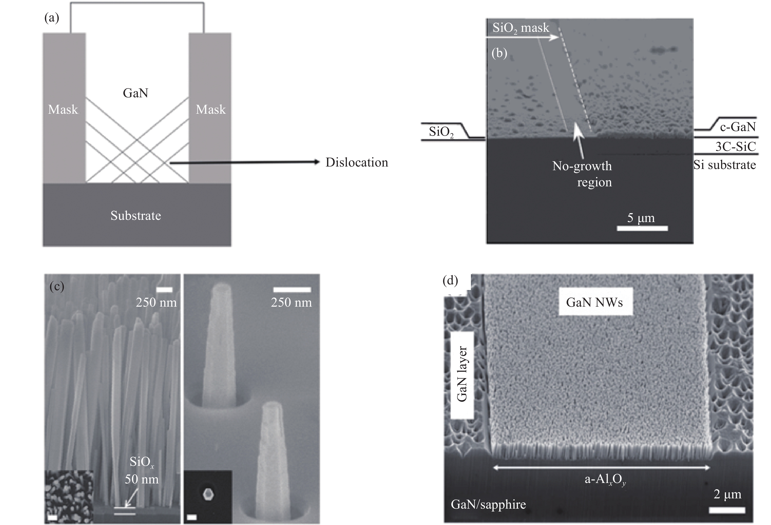
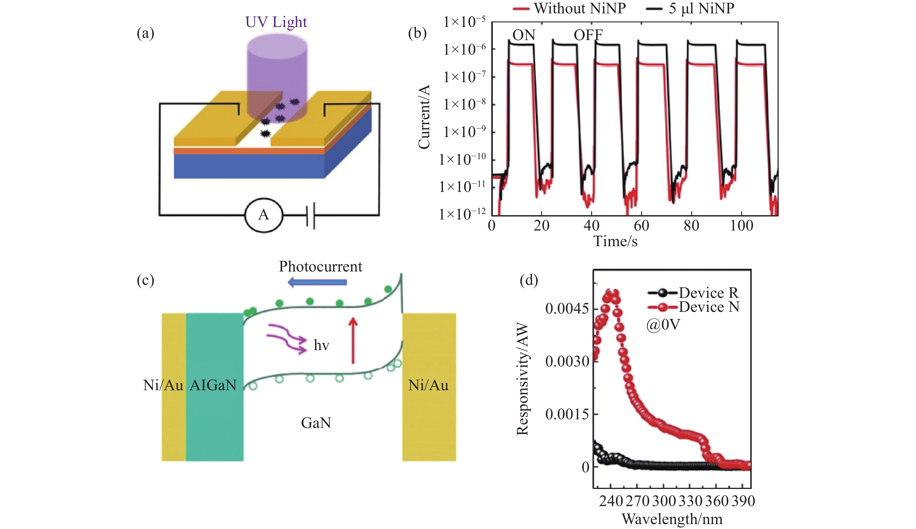
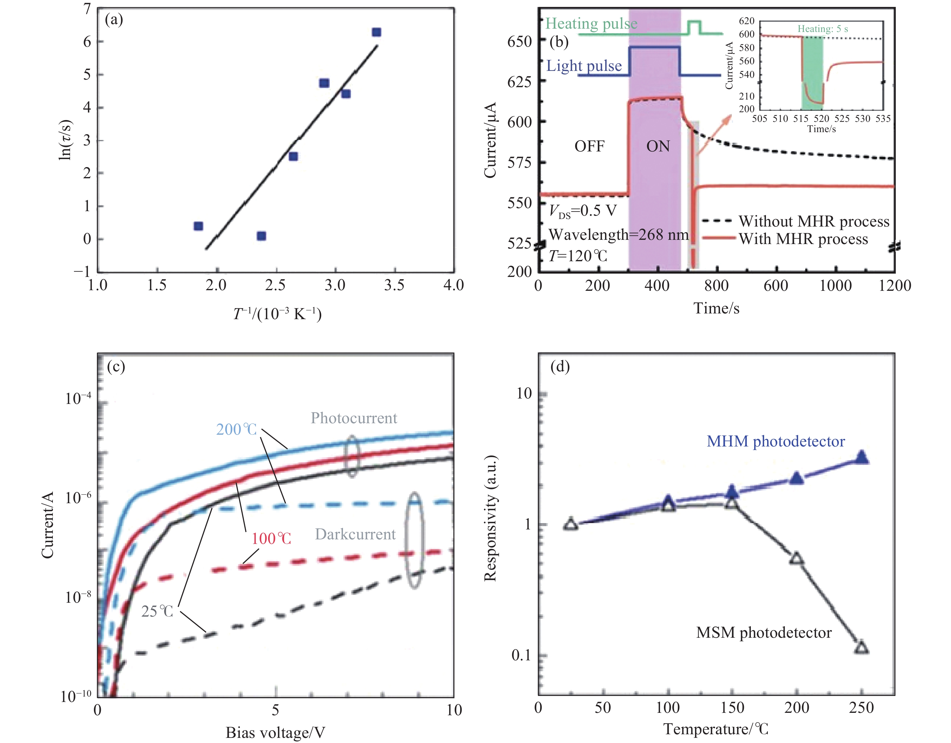
[1] Moses S R, Adorno J J, Palmer A F, et al. Vessel-on-a-chip models for studying microvascular physiology, transport, and function in vitro. Am J Physiol:Cell Physiol, 2021, 320(1): C92 [2] Song W D, Chen J X, Li Z L, et al. Self-powered MXene/GaN van der Waals heterojunction ultraviolet photodiodes with superhigh efficiency and stable current outputs. Adv Mater, 2021, 33 (27): Art No. 2101059 [3] Ding W H, Meng X Q. High performance solar-blind UV detector based on β-Ga2O3/GaN nanowires heterojunction. J Alloys Compd, 2021, 866: Art No. 157564. [4] He T, Zhao Y K, Zhang X D, et al. Solar-blind ultraviolet photodetector based on graphene/vertical Ga2O3 nanowire array heterojunction. Nanophotonics, 2018, 7(9): 1557 doi: 10.1515/nanoph-2018-0061 [5] Jain S K, Aggarwal N, Krishna S, et al. GaN-UV photodetector integrated with asymmetric metal semiconductor metal structure for enhanced responsivity. J Mater Sci Mater Electron, 2018, 29: 8958 doi: 10.1007/s10854-018-8917-3 [6] Yan Z Y, Li S, Yue J Y, et al. Reinforcement of double built-in electric fields in spiro-MeOTAD/Ga2O3/Si p–i–n structure for a high-sensitivity solar-blind UV photovoltaic detector. J Mater Chem C, 2021, 9(41): 14788 doi: 10.1039/D1TC03359J [7] Paskova T, Evans K R. GaN substrates—Progress, status, and prospects. IEEE J Sel Top Quantum Electron, 2009, 15(4): 1041 doi: 10.1109/JSTQE.2009.2015057 [8] Lee W, Lee S, Goto H, et al. Novel buffer layer for the growth of GaN on c-sapphire. Phys Status Solidi C, 2006, 3(6): 1388 doi: 10.1002/pssc.200565410 [9] Waltereit P, Brandt O, Trampert A, et al. Influence of AlN nucleation layers on growth mode and strain relief of GaN grown on 6H–SiC(0001). Appl Phys Lett, 1999, 74(24): 3660 doi: 10.1063/1.123214 [10] Sun Z, Song P F, Nitta S, et al. A-plane GaN growth on (11-20) 4H-SiC substrate with an ultrathin interlayer. J Cryst Growth, 2017, 468: 866 doi: 10.1016/j.jcrysgro.2017.01.031 [11] Feng Y X, Sun H R, Yang X L, et al. High quality GaN-on-SiC with low thermal boundary resistance by employing an ultrathin AlGaN buffer layer. Appl Phys Lett, 2021, 118 (5): Art No. 052104 [12] Arifin P, Sutanto H, Sugianto, et al. Plasma-assisted MOCVD growth of non-polar GaN and AlGaN on Si(111) substrates utilizing GaN-AlN buffer layer . Coatings, 2022, 12(1): Art No. 94 [13] Chen K, Zhang Y C, Zhang J C, et al. Ultrathin GaN film and AlGaN/GaN heterostructure grown on thick AlN buffer by MOCVD. Ceram Int, 2022, 48(24): 36193 doi: 10.1016/j.ceramint.2022.08.176 [14] Kawamura F, Tanpo M, Miyoshi N, et al. Growth of GaN single crystals with extremely low dislocation density by two-step dislocation reduction. J Cryst Growth, 2009, 311(10): 3019 doi: 10.1016/j.jcrysgro.2009.01.125 [15] Shang L, Lu T P, Zhai G M, et al. The evolution of a GaN/sapphire interface with different nucleation layer thickness during two-step growth and its influence on the bulk GaN crystal quality. RSC Adv, 2015, 5(63): 51201 doi: 10.1039/C5RA08369A [16] Woo H, Kim J, Cho S, et al. Epitaxial growth of low temperature GaN using metal migration enhanced epitaxy for high-quality InGaN/GaN heterojunctions. Superlattices Microstruct, 2018, 120: 781 doi: 10.1016/j.spmi.2018.05.048 [17] Liu Y C, Deal M D, Plummer J D. High-quality single-crystal Ge on insulator by liquid-phase epitaxy on Si substrates. Appl Phys Lett, 2004, 84(14): 2563 doi: 10.1063/1.1691175 [18] Park J S, Bai J, Curtin M, et al. Defect reduction of selective Ge epitaxy in trenches on Si(001) substrates using aspect ratio trapping. Appl Phys Lett, 2007, 90(5): Art No. 052113 [19] Suda J D, Kurobe T, Nakamura S, et al. Selective area growth of cubic GaN on 3C-SiC (001) by metalorganic molecular beam epitaxy. Jpn J Appl Phys, 2000, 39(11A): Art No. L1081 [20] Gridchin V O, Reznik R R, Kotlyar K P, et al. Selective-area growth and optical properties of GaN nanowires on patterned SiO x/Si substrates. J Phys: Conf Sers, 2021, 1851(1): Art No. 012006 [21] Sobanska M, Zytkiewicz Z R, Klosek K, et al. Selective area formation of GaN nanowires on GaN substrates by the use of amorphous Al xO y nucleation layer. Nanotechnology, 2020, 31(18): Art No. 184001 [22] Oh J, Ryu J, Yang D, et al. Selective area growth of GaN using polycrystalline γ-Alumina as a mask for fiscrete micro-GaN array. Cryst Growth Des, 2022, 22(3): 1770 doi: 10.1021/acs.cgd.1c01363 [23] Su L X, Yang W, Cai J, et al. Self-powered ultraviolet photodetectors driven by built-in electric field. Small, 2017, 13(45): Art No. 1701687 [24] Su L X, Zhang Q L, Wu T Z, et al. High-performance zero-bias ultraviolet photodetector based on p-GaN/n-ZnO heterojunction. Appl Phys Lett, 2014, 105(7): 072106 doi: 10.1063/1.4893591 [25] Wu Z P, Jiao L, Wang X L, et al. A self-powered deep-ultraviolet photodetector based on an epitaxial Ga2O3/Ga: ZnO heterojunction. J Mater Chem C, 2017, 5(34): 8688 doi: 10.1039/C7TC01741C [26] Xu T, Jiang M M, Wan P, et al. High-performance self-powered ultraviolet photodetector in SnO2 microwire/p-GaN heterojunction using graphene as charge collection medium. J Mater Sci Technol, 2023, 138: 183 doi: 10.1016/j.jmst.2022.07.050 [27] Zhang Y, Chen J, Zhu L, et al. Self-powered high-responsivity photodetectors enhanced by the pyro-phototronic effect based on a BaTiO3/GaN heterojunction. Nano Lett, 2021, 21(20): 8808 doi: 10.1021/acs.nanolett.1c03171 [28] Yan M N, Yu N S, Du S Y, et al. A self-powered ZnO nanoarrays/GaN heterojunction ultraviolet photodetectors grown on Si(111) substrate. Bull Mater Sci, 2022, 45(3): 105 doi: 10.1007/s12034-022-02679-4 [29] Macaluso R, Lullo G, Crupi I, et al. Progress in violet light-emitting diodes based on ZnO/GaN heterojunction. Electronics, 2020, 9(6): Art No. 991 [30] Mishra M, Gundimeda A, Garg T, et al. ZnO/GaN heterojunction based self-powered photodetectors: Influence of interfacial states on UV sensing. Appl Surf Sci, 2019, 478: 1081 doi: 10.1016/j.apsusc.2019.01.192 [31] Song W Q, Dai X B, He Y K, et al. The gold nanoparticles enhanced ZnO/GaN UV detector. IEEE J Electron Devices Soc, 2022, 10: 847 doi: 10.1109/JEDS.2022.3212395 [32] Zhou H, Gui P B, Yang L, et al. High performance, self-powered ultraviolet photodetector based on a ZnO nanoarrays/GaN structure with a CdS insert layer. New J Chem, 2017, 41(12): 4901 doi: 10.1039/C7NJ01140G [33] Huang Y, Zhang L C, Wang J B, et al. Enhanced photoresponse of n-ZnO/p-GaN heterojunction ultraviolet photodetector with high-quality CsPbBr3 films grown by pulse laser deposition. J Alloys Compd, 2019, 802: 70 doi: 10.1016/j.jallcom.2019.06.215 [34] Peng Y Y, Lu J F, Wang X D, et al. Self-powered high-performance flexible GaN/ZnO heterostructure UV photodetectors with piezo-phototronic effect enhanced photoresponse. Nano Energy, 2022, 94: Art No. 106945 [35] Feng S Y, Liu Z T, Feng L Z, et al. High-performance self-powered ultraviolet photodetector based on Ga2O3/GaN heterostructure for optical imaging. J Alloys Compd, 2023, 945: Art No. 169274 [36] Ding S, Chen K, Xiu X Q, et al. Self-powered solar-blind photodetectors based on vertically aligned GaN@ Ga2O3 core–shell nanowire arrays. ACS Appl Nano Mater, 2022, 5(10): 14470 doi: 10.1021/acsanm.2c02836 [37] Ma Y J, Chen T W, Zhang X D, et al. High-photoresponsivity self-powered a-, ε-, and β-Ga2O3/p-GaN heterojunction UV photodetectors with an in situ GaON layer by MOCVD. ACS Appl Mater Interfaces, 2022, 14(30): 35194 doi: 10.1021/acsami.2c06927 [38] Park C H, Zhang S B, Wei S H. Origin of p-type doping difficulty in ZnO: The impurity perspective. Phys Rev B, 2002, 66(7): 073202 doi: 10.1103/PhysRevB.66.073202 [39] Lin Z L, Lin T T, Lin T J, et al. Ultrafast response self-powered UV photodetectors based on GaS/GaN heterojunctions. Appl Phys Lett, 2023, 122 (13): Art No. 131101 [40] Jiang H H, Zhang Y , Li X, et al. GaN MSM structure UV photodetector detector based on nonplanar Si substrate and its performance optimization. Semicond Sci Technol, 2022, 37(10): Art No. 105020 [41] An Y J, Liao J, Wu C, et al. GaN MSM UV detectors with different electrode materials. IEEE J Electron Devices Soc, 2021, 9: 1210 doi: 10.1109/JEDS.2021.3106097 [42] Nallabala N K R, Reddy V R M, Singh V R, et al. Enhanced photoresponse performance in GaN based symmetric type MSM ultraviolet-A and MIS ultraviolet-A to C photodetectors. Sens Actuat A: Phys, 2022, 339: Art No. 113502 [43] Yang G F, Li Y H, Liu Y S, et al. Surface modification of AlGaN solar-blind ultraviolet MSM photodetectors with octadecanethiol. IEEE Trans Electron Devices, 2021, 69(1): 195 [44] Berger P R. Metal-semiconductor-metal photodetectors//Symposium on Integrated Optics, San Jose, 2001 [45] Aggarwal N, Krishna S, Sharma A, et al. A highly responsive self-driven UV photodetector using GaN nanoflowers. Adv Electron Mater, 2017, 3(5): Art No. 1700036 [46] Freeouf J F, Jackson T N, Laux S E, et al. Effective barrier heights of mixed phase contacts: Size effects. Appl Phys Lett, 1982, 40(7): 634 doi: 10.1063/1.93171 [47] Teker K, Hocaoglu A, Yildirim M A. Improving detectivity of self-powered GaN ultraviolet photodetector by nickel nanoparticles. Appl Phys B, 2021, 127: Art No. 7 [48] Amendola V, Pilot R, Frasconi M, et al. Surface plasmon resonance in gold nanoparticles: a review. J Phys: Condens Matter, 2017, 29(20): Art No. 203002 [49] Chen J N, Albella P, Pirzadeh Z, et al. Plasmonic nickel nanoantennas. Small, 2011, 7(16): 2341 doi: 10.1002/smll.201100640 [50] Wang J X, Chu C S, Tian K K, et al. Polarization assisted self-powered GaN-based UV photodetector with high responsivity. Photon Res, 2021, 9(5): Art No. 734 [51] Li J Z, Lin J Y, Jiang H X, et al. Persistent photoconductivity in a two-dimensional electron gas system formed by an AlGaN/GaN heterostructure. J appl phys, 1997, 82(3): 1227 doi: 10.1063/1.365893 [52] Hou M M, So H, Suria A J, et al. Suppression of persistent photoconductivity in AlGaN/GaN ultraviolet photodetectors using in situ heating. IEEE Electron Device Lett, 2017, 38(1): 56 doi: 10.1109/LED.2016.2626388 [53] Qiu C H, Pankove J I. Deep levels and persistent photoconductivity in GaN thin films. Appl phys lett, 1997, 70(15): 1983 doi: 10.1063/1.118799 [54] Sun J W, Zhang S, Zhan T, et al. A high responsivity and controllable recovery ultraviolet detector based on a WO3 gate AlGaN/GaN heterostructure with an integrated micro-heater. J Mater Chem C, 2020, 8(16): 5409 doi: 10.1039/D0TC00553C [55] Tang X, Ji F W, Wang H, et al. Temperature enhanced responsivity and speed in an AlGaN/GaN metal-heterostructure-metal photodetector. Appl Phys Lett, 2021, 119(1): Art No. 013503 [56] Jiang Z Y, Atalla M R M, You G J, et al. Monolithic integration of nitride light emitting diodes and photodetectors for bi-directional optical communication. Opt Lett, 2014, 39(19): 5657 doi: 10.1364/OL.39.005657 [57] Lyu Q, Jiang H, Lau K M. Monolithic integration of ultraviolet light emitting diodes and photodetectors on a p-GaN/AlGaN/GaN/Si platform. Opt Express, 2021, 29(6): 8358 doi: 10.1364/OE.418843 [58] Brubaker M D, Blanchard P T, Schlager J B, et al. On-chip optical interconnects made with gallium nitride nanowires. Nano Lett, 2013, 13(2): 374 doi: 10.1021/nl303510h [59] Tchernycheva M, Messanvi A, de Luna Bugallo A, et al. Integrated photonic platform based on InGaN/GaN nanowire emitters and detectors. Nano Lett, 2014, 14(6): 3515 doi: 10.1021/nl501124s [60] Wang B, Liang S H, Yu J C, et al. Cascade GaN-based micro-photodiodes for photonic integration. J Phys D: Appl Phys, 2022, 55(40): Art No. 404004 [61] Shi J Y, Xu Z Y, Niu W Q, et al. Si-substrate vertical-structure InGaN/GaN micro-LED-based photodetector for beyond 10 Gbps visible light communication. Photon Res, 2022, 10(10): 2394 doi: 10.1364/PRJ.465455 -

 下载:
下载:

 点击查看大图

图(7)
计量
- 文章访问数: 122
- HTML全文浏览量: 60
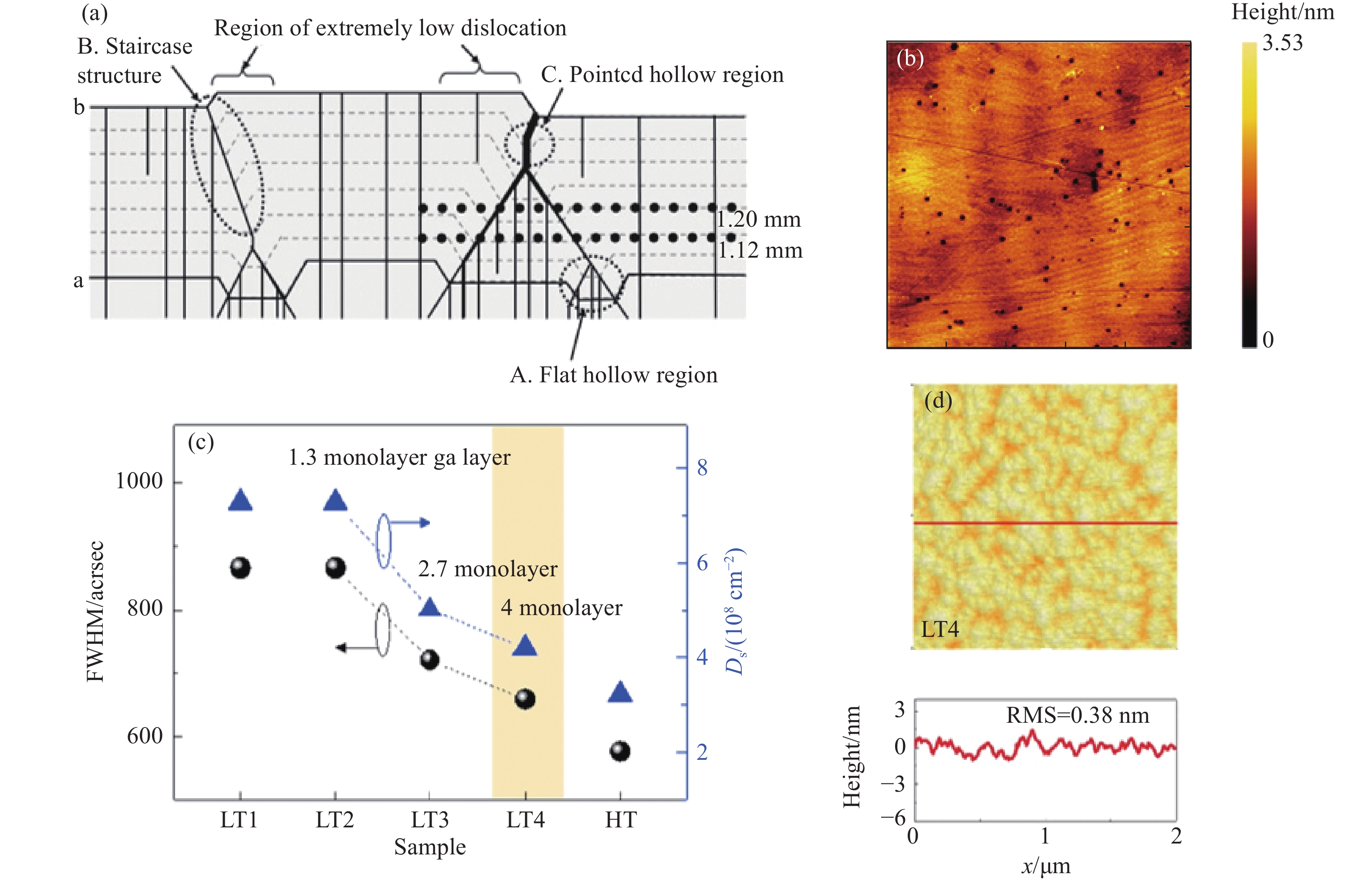
- PDF下载量: 45
- 被引次数: 0
